Bridging the analog gap
The investigations up to this point remained entirely in the digital domain. Waveforms like the ones shown in the VLM5030 gate-level design validation and lock-step comparison post were derived from the PCM data right before it enters the DAC. This is most suitable to obtain precise information about the cycle behaviour of the design but neglects the final conversion step from digital to the analog output at the DAO pin.
What is the DAC’s transfer function, and most importantly: Is it linear or logarithmic?
DAC architecture
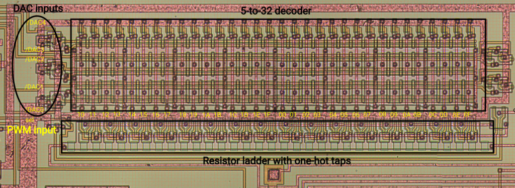
Let’s have a look at the DAC layout.
It’s partitioned into 4 sub-circuits:
- 5 inputs to the DAC (/DAC[4:0])
- The 5-to-32 decoder with a regular ROM-like structure
- 34 resistors chained up (light green rectangles) and tapped by 2x 32 transistors
- A Y-shaped output MUX for the PWM overlay, controlled by sel input
- Output buffer for DAO pin (not visible in the picture above)
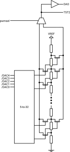
The schematic on the right shows the simplified circuit. Note that the PWM overlay is not included.
Based on the schematic we can conclude that the DAC is linear if the values of the 34 resistors are equal. They obviously share the same geometry, but electrical characteristics cannot be obtained from the die shot. Some measurement is needed to clarify details.
Testability considerations
Testing the DAC requires controllability of /DAC[4:0] inputs and observability at the DAC output.
DAC observation in a packaged chip
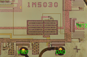
Starting with the output, there are two options for measuring – at the DAO pin or the TST2 pin. TST2 would be preferable as it provides direct access to the internal node, even allowing to measure resistances directly. Unfortunately, the TST2 pad is not bonded on my chip. The missing bond is also visible in the die shot – there’s only the scrub mark from wafer probing but no bond wire.
DAO is the only feasible observation point.
DAC control with DFT
The situation for control at /DAC[4:0] is more complex since they are internal signals that are computed from the frame parameters. Furthermore, they are highly dynamic, rendering a static output voltage measurement almost unfeasible as a close correlation between input value and output voltage is required.
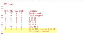
DFT to the rescue – Sanyo fortunately added test features in the design that come in handy:
Enabling TST1 while keeping VREF & START at low activates the DAC test mode that propagates the D[7:0] input bus to /DAC[4:0]. Internally, the frame decoder and register file are bypassed (ID bus) as well as the arithmetic unit that drives onto the IE bus. This test mode also bypasses the register stage for synchronizing the calculated values towards the DAC inputs with the sample rate.
In summary, we get full control over /DAC[4:0] from external pins without the need to sync to any clock!
Measurement
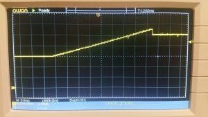
The final measurement setup is straight forward now. A modified FSM inside the test rig activates the DAC test mode and linearly sweeps the DAC inputs while the output voltage is captured at DAO.
The resulting ramp confirms the initial assumption that the transfer function of the DAC is indeed linear.
Analysis and a hypothesis
What could cause that the VLM5030 partially behaves non-deterministic for certain frames? The usual suspects are incomplete reset and …randomness. Lots of internal states / flip-flops aren’t affected by the RST input, so that could be a cause for repeated execution of the same speech sample. The random source is not strictly random, however. It’s an LFSR and as such it has a fixed sequence of 0s & 1s and is thus fully deterministic when starting from a known initial value. It’s even reset by RST, so what could go wrong?
Simulation
The issue is 100% reproducible in a controlled environment and the time slots of the variations are fixed. Ideal boundary conditions to take this back to simulation for further investigation.
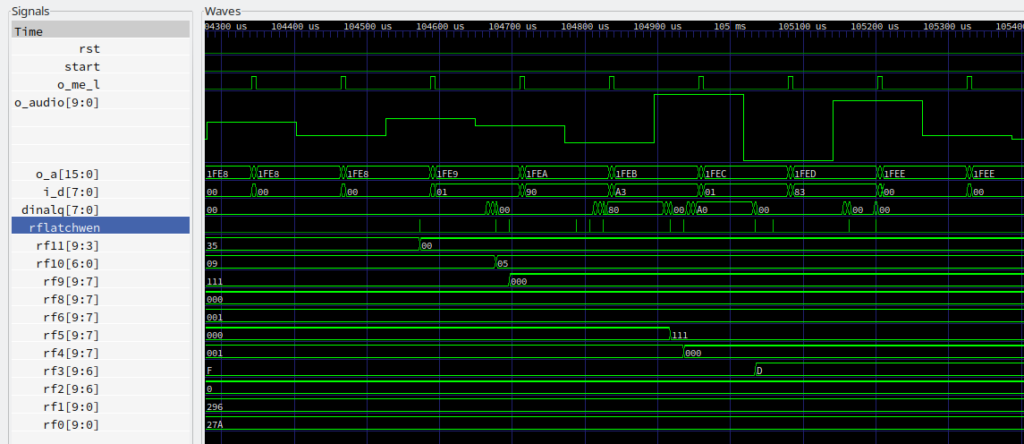
Simulation output above shows that the VLM reads the next frame from address 0x1FF8 at 104.5 ms. This frame loads 0x00 into registerfile slot 11 (rf11[9:3]) that stores the frame’s pitch information. Pitch value 0x00 configures noise generation which makes use of the random generator (ref. vlm5030.cpp L.58). Time to take a closer look at this circuit.
Design analysis and hypothesis
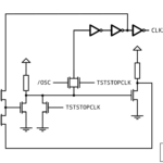
Revisiting Randomness on a microscopic level, look at note at the bottom of the schematic that says “NOTE: Active RST shifts 0 into the LFSR.” Contemplate on the term “shifts”, it means that the LFSR is reset synchronously when RST is active. Coincidentally, the entire clocking system is halted during RST:
So no matter for how long RST is kept active, there won’t be a clock to clear the LFSR.
Looks like the non-determinism might be caused by the missing reset of the LFSR when the speech sample starts. The LFSR itself is fully deterministic but its starting state is random at the time when the speech sample starts. The LFSR’s current state is not controllable under real world conditions.
Definition of experiment
What if the LFSR gets cleared at the beginning of a speech sample? This appears to be the original intention of the design.
The chip can’t be changed of course, but we can run this experiment with the gate-level design.
Running the asynchronous version in the test rig multiple times results in exactly the same waveform for each run.
Seems like the designers had everything in shape except for the indisposition to expect synchronous reset during a mode where all clocks are stopped. Does this mean the chip itself would also change to deterministic behaviour? Likely, but without actually changing the chip’s logic we have a strong indication but not a proof.
Conclusion
The chip produces different waveforms for noise frames when re-running the same speech sample. This difference is very likely caused by the LFSR in the random source:
- The LFSR chain is cleared synchronously by RST
- Clocks are disabled during RST
- Thus the LFSR’s synchronous reset is not effective due to missing clock
VLM5030 gate-level design validation and lock-step comparison
Now with the extracted gate-level design in place, how does it perform?
The initial validation consisted of two basic phases:
- VHDL simulation in a test bench that dumps the PCM audio to a binary file. The binary is imported with Audacity and converted to WAV format for listening.
Goal: Prove that the design can actually generate correct samples in a flexible environment. - Integration of the gate-level design in several Konami FPGA conversions like Track’n’Field, Hypersports, Yie-Ar-Kung-Fu and others
Goal: Prove that the design interfaces correctly with the target systems and compare audio with real hardware.
Each method has its pros and cons. Simulation enables maximum controllability and observability of internal signals, but its execution speed is slow and variation of input is limited. Running the replacement in FPGA conversions adds variation in terms of system interfacing and sample/function coverage but offers almost zero control and observe features. One can just run the game and listen to the samples that are played in attract mode or in the first few levels.
To bridge both worlds, I created a test rig consisting of a small Cyclone II board that contains the gate-level replacement plus the ROM and also controls an external VLM5030 chip. It enables full control over the selection of speech samples without the need to trigger specific in-game situations.
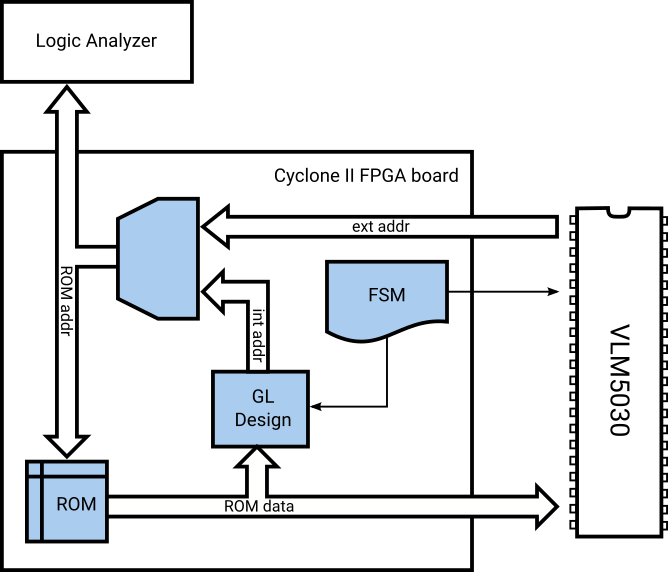
Block diagram of the VLM5030 test rig
Operation of the chip and the replacement is observed by a logic analyzer that’s hooked to the address bus. This makes use of VLM5030’s feature to output audio as 10 bit signed integer PCM samples on the address bus. Tracing both the chip’s and the replacement’s audio stream from a common trigger enables direct comparison of their PCM output with sample rate granularity.
The results are quite impressing – the screenshot below shows a range of Salamander’s “Destroy them all!” speech sample. Topmost channel is the gate-level design, followed by the chip and a re-run of the chip as the bottom channel. They’re perfectly in sync and sample values appear to match as well!

Detail of Salamander’s “Destroy them all!” at 20 ms. From top to bottom: GL design, VLM5030, VLM5030 2nd run
However, there are locations where all three waveforms begin to diverge (around the 0.108 s mark). It’s not necessarily just a difference between the gate-level design and the chip, but also the chip produces a different waveform during its 2nd run:

Detail of Salamander’s “Destroy them all!” at 100 ms. From top to bottom: GL design, VLM5030, VLM5030 2nd run
All three converge later at the 0.270 s mark and continue in lock-step:

Detail of Salamander’s “Destroy them all!” at 255 ms. From top to bottom: GL design, VLM5030, VLM5030 2nd run
Conclusion
Initial comparison results show that the gate-level design produces identical audio waveforms for most of the frames. It differs during frames where the chip itself exhibits seemingly non-deterministic behaviour. In addition, the gate-level design also shows such behaviour and produces different waveforms during repeated runs of the same sample. Further analysis is required to understand this in more detail.
References
Gate-level replacement: salamander_gl.wav
VLM5030 chip: salamander_chip.wav
VLM5030 chip, 2nd run: salamander_chip_2ndrun.wav
Extract, reconstruct, simulate … repeat
When I started to search for the random generator the first challenge was the decision where to begin with. Looking at the die, there are not many landmarks that provide clear guidance. The ROMs are quite prominent due to their regular structure, but they don’t have a direct relationship to the random generator. Furthermore, the purpose of two of the three ROMs was entirely unclear.
Next on the list of obvious items are the pads of course. They neatly follow the DIP40 pin-out and are assigned to functions in no time. Should I start off from the data or address bus? That would mean to dig through data paths whereas I expected the random generator to be located in a processing or calculation block. Somewhere in the middle between K-factors and final PCM output. With potentially deep logic cones on either side, not an appealing idea. I briefly considered entering the design via the few control pins, but the perspective to untangle piles of potentially complex control logic wasn’t appealing at all.
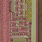 In the end I decided for tracing the clock tree first. That’s a single source signal, easy to identify from the pads, and – if Sanyo designed a reasonable clock system – fans out to all function blocks. I also hoped that the logic in the clock tree is less complex and that the purpose of such logic is easy to understand.
The OSC2 pin feeds directly into the clock generation system where the 3.58 MHz clock is divided by 2 before being used anywhere else. Identifying the divider was my first lesson in tracing logic from the die shot. After much back and forth I figured that all these polygons are just standard logic gates – and that they actually make sense. I mean, it’s located in the center of the die, and a /2 divider can be expected at the clock tree’s root.
Curiosity was fueled enough to tackle further gates in the neighbourhood to the divider. This time I faced a number of flip-flops – they look different than the logic gates but once I understood the concept of 2-phase clocking and latch/feedback topology, they turned out to be positive edge triggered D-type registers arranged in a shift chain with feedback. Not too bad for starters, but isn’t that a bit too easy? Let’s build it a VHDL model and check the extracted circuit in simulation. The waveforms from simulation backed the extraction result: That shift chain generates 10+ staggered clocks.
Step by step I paved my way through the design (still searching for the random source):
- Extract the gates of a sub-circuit
- Reconstruct the sub-circuit as a VHDL model based on the extraction result
- Simulate the model to examine its behaviour and to validate the extraction
- Repeat with the next sub-circuit
At the point when the random source had been identified, I looked back at quite a collection of models running nicely in simulation. Should I stop here or keep on moving until I would hit a wall maybe?
TLDR; I decided to continue, repeatedly cycled through above steps and didn’t hit any walls. The VLM5030 gate-level replacement is available at FPGAArcade’s github repo.
